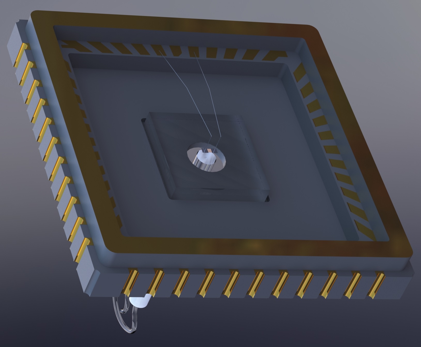
UCPH demonstrator package design
In addition to the study, fabrication and experimental test on optomechanical nanostructures, HOT has the aim to demonstrate the feasibility of fabricating and packaging prototype HOT-devices exploiting standard methods of the CMOS-industry, including Silicon photonics. While unconventional processing is not a priori a show-stopper for commercialization, the ability to utilize standard processes opens the door to massively parallel batch processing, a requirement for consumer market applications in large volumes. The packaging activity will be based on both Ceramic and Organic base structures for the package. Both technologies represent a standard in every sector of microelectronics and optics. The first one is mainly used for obtaining full hermetic enclosure and good reliability in respect to harsh environments, and the second is very advantageous both in terms of development and unit level production costs. Finally three prototypes are undergoing packaging activity. In all ,special attention has been payed to redesigning structures on the chip to allow automatic fibre block alignment. Process wise, the peculiarity of one of the prototypes is leading to the need to use a low melting temperature solder paste for component sealing.
The fabrication is based on a standard silicon photonics platform, with the design adapted to allow for release of the opto-mechanical devices. Two relevant prototypes designed by WP3 partners were selected and submitted to the fab. One has been fabricated and is currently under testing. The second one will be completed during the final year of the project.